- 您现在的位置:买卖IC网 > Sheet目录3890 > PIC16C717T-E/SS (Microchip Technology)IC MCU OTP 2KX14 A/D PWM 20SSOP
2002 Microchip Technology Inc.
DS41120B-page 107
PIC16C717/770/771
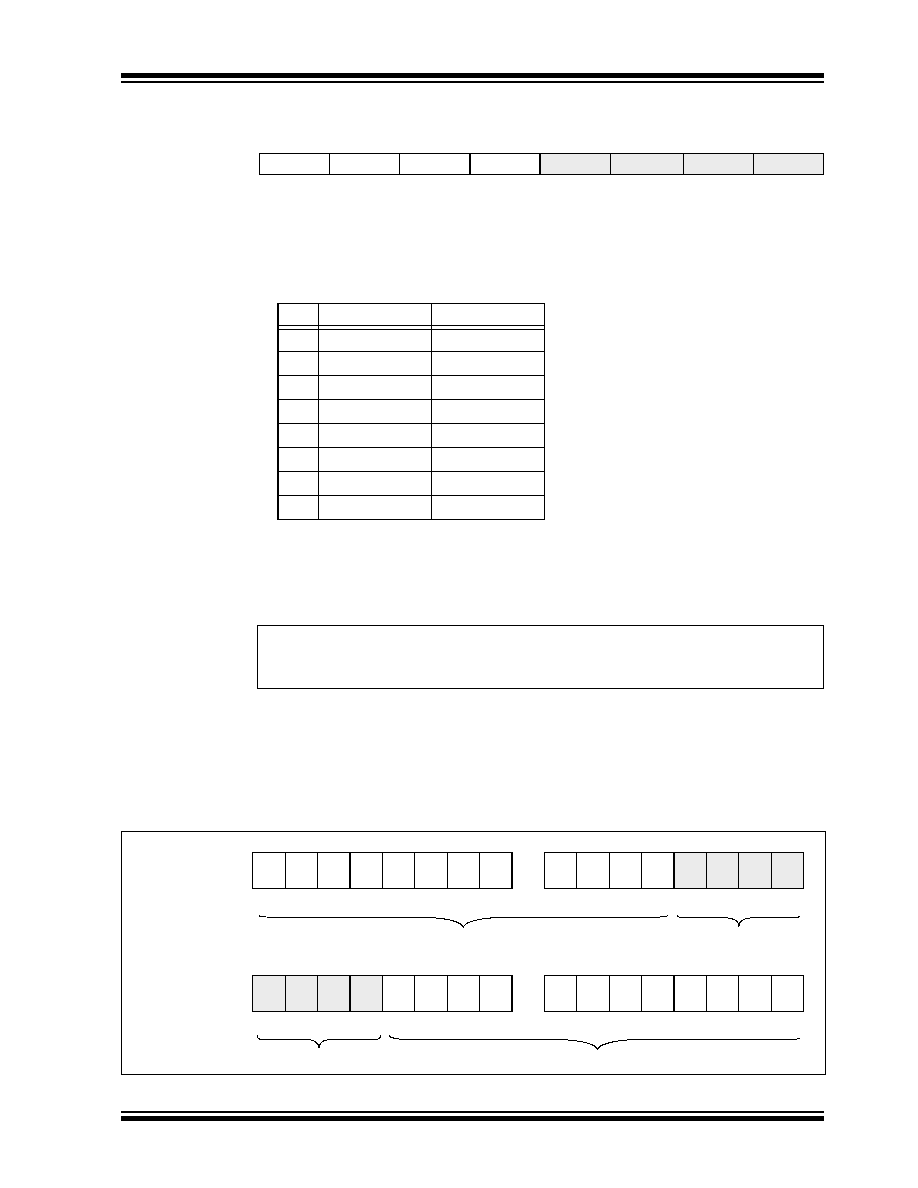
REGISTER 11-2:
A/D CONTROL REGISTER 1 (ADCON1: 9Fh)
The value that is in the ADRESH and ADRESL regis-
ters are not modified for a Power-on Reset. The
ADRESH and ADRESL registers will contain unknown
data after a Power-on Reset.
The A/D conversion results can be left justified (ADFM
bit cleared), or right justified (ADFM bit set).
Figure 11-1 through Figure 11-2 show the A/D result
data format of the PIC16C717/770/771.
FIGURE 11-1: PIC16C770/771 12-BIT A/D RESULT FORMATS
R/W-0
ADFM
VCFG2
VCFG1
VCFG0
Reserved
Reserved Reserved
bit 7
bit 0
bit 7
ADFM: A/D Result Format Select bit
1
= Right justified
0
= Left justified
bit 6-4
VCFG<2:0>: Voltage Reference Configuration bits
bit 3-0
Reserved: Do not use.
Note 1: This parameter is VDD for the PIC16C717.
2: This parameter is VSS for the PIC16C717.
Legend:
R = Readable bit
W = Writable bit
U = Unimplemented bit, read as ‘0’
- n = Value at POR
’1’ = Bit is set
’0’ = Bit is cleared
x = Bit is unknown
A/D VREF+A/D VREF-
000
AVDD(1)
AVSS(2)
001
External VREF+
External VREF-
010
Internal VRH
Internal VRL
011
External VREF+AVSS(2)
100
Internal VRH
AVSS(2)
101
AVDD(1)
External VREF-
110
AVDD(1)
Internal VRL
111
Internal VRL
AVSS
ADRESH (1Eh)
ADRESL (9Eh)
Left Justified
(ADFM = 0)
MSB
LSB
bit7
12-bit A/D Result
Unused
Right Justified
(ADFM = 1)
MSB
LSB
bit7
Unused
12-bit A/D Result
发布紧急采购,3分钟左右您将得到回复。
相关PDF资料
PIC16LC770T-E/SO
IC MCU OTP 2KX14 A/D PWM 20SOIC
PIC16C771T/SO
IC MCU OTP 4KX14 A/D PWM 20SOIC
PIC16LC717T-I/SS
IC MCU OTP 2KX14 A/D PWM 20SSOP
PIC16C717T/SS
IC MCU OTP 2KX14 A/D PWM 20SSOP
PIC16LC770T-I/SO
IC MCU OTP 2KX14 A/D PWM 20SOIC
PIC16LC771T-E/SS
IC MCU OTP 4KX14 A/D PWM 20SSOP
PIC16C771T-E/SS
IC MCU OTP 4KX14 A/D PWM 20SSOP
PIC16LC771T-I/SO
IC MCU OTP 4KX14 A/D PWM 20SOIC
相关代理商/技术参数
PIC16C717T-I/SO
功能描述:8位微控制器 -MCU 3.5KB 256 RAM 16 I/O RoHS:否 制造商:Silicon Labs 核心:8051 处理器系列:C8051F39x 数据总线宽度:8 bit 最大时钟频率:50 MHz 程序存储器大小:16 KB 数据 RAM 大小:1 KB 片上 ADC:Yes 工作电源电压:1.8 V to 3.6 V 工作温度范围:- 40 C to + 105 C 封装 / 箱体:QFN-20 安装风格:SMD/SMT
PIC16C717T-I/SS
功能描述:8位微控制器 -MCU 3.5KB 256 RAM 16 I/O RoHS:否 制造商:Silicon Labs 核心:8051 处理器系列:C8051F39x 数据总线宽度:8 bit 最大时钟频率:50 MHz 程序存储器大小:16 KB 数据 RAM 大小:1 KB 片上 ADC:Yes 工作电源电压:1.8 V to 3.6 V 工作温度范围:- 40 C to + 105 C 封装 / 箱体:QFN-20 安装风格:SMD/SMT
PIC16C71T-04/SO
功能描述:8位微控制器 -MCU 1.75KB 36 RAM 13 I/O 4MHz SOIC18 RoHS:否 制造商:Silicon Labs 核心:8051 处理器系列:C8051F39x 数据总线宽度:8 bit 最大时钟频率:50 MHz 程序存储器大小:16 KB 数据 RAM 大小:1 KB 片上 ADC:Yes 工作电源电压:1.8 V to 3.6 V 工作温度范围:- 40 C to + 105 C 封装 / 箱体:QFN-20 安装风格:SMD/SMT
PIC16C71T-04I/SO
功能描述:8位微控制器 -MCU 1.75KB 36 RAM 13 I/O 4MHz Ind Temp SOIC18 RoHS:否 制造商:Silicon Labs 核心:8051 处理器系列:C8051F39x 数据总线宽度:8 bit 最大时钟频率:50 MHz 程序存储器大小:16 KB 数据 RAM 大小:1 KB 片上 ADC:Yes 工作电源电压:1.8 V to 3.6 V 工作温度范围:- 40 C to + 105 C 封装 / 箱体:QFN-20 安装风格:SMD/SMT
PIC16C71T-20/SO
功能描述:8位微控制器 -MCU 1.75KB 36 RAM 13 I/O RoHS:否 制造商:Silicon Labs 核心:8051 处理器系列:C8051F39x 数据总线宽度:8 bit 最大时钟频率:50 MHz 程序存储器大小:16 KB 数据 RAM 大小:1 KB 片上 ADC:Yes 工作电源电压:1.8 V to 3.6 V 工作温度范围:- 40 C to + 105 C 封装 / 箱体:QFN-20 安装风格:SMD/SMT
PIC16C71T-20I/SO
功能描述:8位微控制器 -MCU 1.75KB 36 RAM 13 I/O RoHS:否 制造商:Silicon Labs 核心:8051 处理器系列:C8051F39x 数据总线宽度:8 bit 最大时钟频率:50 MHz 程序存储器大小:16 KB 数据 RAM 大小:1 KB 片上 ADC:Yes 工作电源电压:1.8 V to 3.6 V 工作温度范围:- 40 C to + 105 C 封装 / 箱体:QFN-20 安装风格:SMD/SMT
PIC16C72/JW
功能描述:8位微控制器 -MCU 3.5KB 128 RAM 22 I/O RoHS:否 制造商:Silicon Labs 核心:8051 处理器系列:C8051F39x 数据总线宽度:8 bit 最大时钟频率:50 MHz 程序存储器大小:16 KB 数据 RAM 大小:1 KB 片上 ADC:Yes 工作电源电压:1.8 V to 3.6 V 工作温度范围:- 40 C to + 105 C 封装 / 箱体:QFN-20 安装风格:SMD/SMT
PIC16C72-04/SO
功能描述:8位微控制器 -MCU 3.5KB 128 RAM 22 I/O RoHS:否 制造商:Silicon Labs 核心:8051 处理器系列:C8051F39x 数据总线宽度:8 bit 最大时钟频率:50 MHz 程序存储器大小:16 KB 数据 RAM 大小:1 KB 片上 ADC:Yes 工作电源电压:1.8 V to 3.6 V 工作温度范围:- 40 C to + 105 C 封装 / 箱体:QFN-20 安装风格:SMD/SMT